Product categories
News center
Contact us
- Add: 2F, Building 6, Software Park Zone B, Gulou District, Fuzhou, Fujian, China
- Tel: 0591-22628762
- Fax: 0591-22628951
- Postal Code: 350001
- Email: info@fzhokin.com
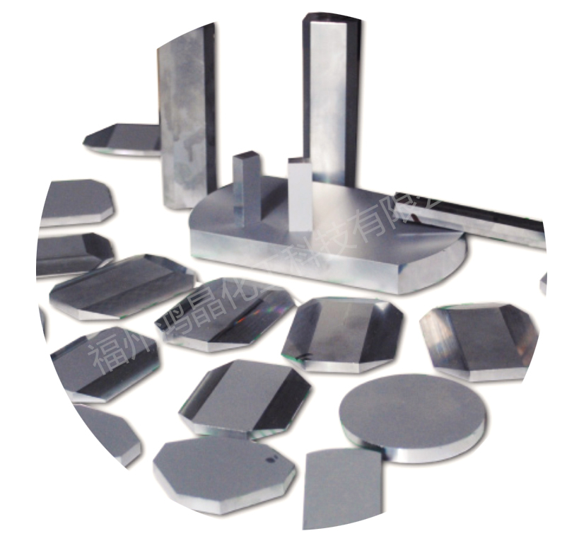
Product Numbers:OG-silicon wafer
Product introduction: Monocrystalline silicon is a kind of infrared optical material with excellent comprehensive price ratio. It is used to make infrared optical lenses. It is mainly used in high-tech fields such as thermal imaging system, forward-looking infrared, mobile sensors and so on. Compared with other mirror materials such as copper and molybdenum, monocrystalline silicon has many advantages, such as good thermal conductivity, excellent thermal stability, low thermal expansion coefficient, relatively low density, low cost and easy precision processing.At present, it is the preferred base material for carbon dioxide laser mirrors.
Optical characteristics:
Czochralski monocrystalline silicon(CZ) has a strong oxygen absorption peak at 9.1 um. When used as a transmission level material, it is mainly used in the 3-5 um band of the first infrared optical window.The thickness of Czochralski single crystal silicon has little effect on the optical transmittance in 1.2-6.7 um band, and its average infrared transmittance is over 50%.
Because the oxygen content of zone melted silicon(FZ) is much lower than that of CZ silicon, the infrared transmittance curve of FZ silicon is fairly straight, so it can be used in the second infrared window 7-14 um band. The thickness of components in this band becomes the key parameter affecting the optical transmittance. The average optical transmittance of CZ silicon with thickness less than 1 mm is more than 50%.
Optical characteristic parameters:
Transmission Range : 1.2 to 15 microns
Refractive Index : 3.4223 at 5 microns
Reflection Loss : 51.0% at 5 microns(2 surfaces)
Index of Absorption : 1x10⁻³cm-1 at 3 microns
dN/dT : 160x10-6/℃
dN/dμ : 10.4 microns
Product Specification:
Classification of Crystal Growth Mode :MCZ-Si FZ-Si
Classification of Crystal Directions :100 111
Type Classification of Doping Elements :Type N Type p
Purity : >99.999%(5N)
Resistivity : 1-100Ω·cm
Shape :Arbitrary Customization
Optical grade single crystal silicon requires not only high purity of materials, but also strict processing accuracy of materials. Our company is based on long-term processing experience, precise processing equipment and good testing methods. It can process all kinds of silicon optical components with high requirements of shape and accuracy, and can meet all kinds of harsh requirements.


 Record No.35010202000884 of public security organs.